Question
In: Physics
Draw the following circuits: a. (1 pt) What is the purpose of a rectifier circuit? b....
Draw the following circuits:
a. (1 pt) What is the purpose of a rectifier circuit?
b. (2 pts) Half
Solutions
Expert Solution
A)
The very purpose of the rectifier is to convert AC to steady
DC.
The basic components used in the rectifier circuits are
Transformer(step down) ,diodes, capacitors, inductors and
resistors.
If only one diode is used it is called a half wave rectifier.
Though it converts AC into DC , this DC will not be a perfect DC.
because the bi-directional current is converted into a
unidirectional, intermittant current. Of course this can be
smoothened to certain extent by using suitable capacitors. or some
other components.
At the same time , if two diodes are used
both the half cycles of the AC will be utilised to produce a better
and more effective DC.This is called a full wave rectifier. To
reduce the fluctuations, again suitable components of the
appropriate value can be used in the filter circuit. Nowadays very
efficient ICs are in the market in place of these components.
B) Half-wave rectifier -- used when regulation and ripple voltage of the DC output is non-critical
Half Wave Rectifier:
The half wave rectifier is a type of rectifier that rectifies only half cycle of the waveform. This article describes the half wave rectifier circuit working. The half rectifier consist a step down transformer, a diode connected to the transformer and a load resistance connected to the cathode end of the diode. The circuit diagram of half wave transformer is shown below:
![]()

The main supply voltage is given to the transformer which will increase or decrease the voltage and give to the diode. In most of the cases we will decrease the supply voltage by using the step down transformer here also the output of the step down transformer will be in AC. This decreased AC voltage is given to the diode which is connected serial to the secondary winding of the transformer, diode is electronic component which will allow only the forward bias current and will not allow the reverse bias current. From the diode we will get the pulsating DC and give to the load resistance RL.
C)
The full wave rectifier can be further divided mainly into following types.
- Center Tapped Full Wave Rectifier
- Full Wave Bridge Rectifier
Center Tapped Full Wave Rectifier:
Center tap is the contact made at the middle of the winding of the transformer.
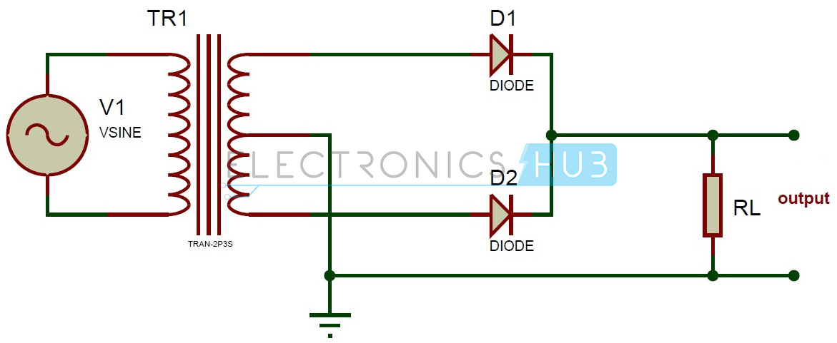
Center Tapped Full Wave Rectifier Circuit Diagram
In the center tapped full wave rectifier two diodes were used. These are connected to the center tapped secondary winding of the transformer. Above circuit diagram shows the center tapped full wave rectifier. It has two diodes. The positive terminal of two diodes is connected to the two ends of the transformer. Center tap divides the total secondary voltage into equal parts.
Center Tapped Full Wave Rectifier Working:
The primary winding of the center tap transformer is applied with the Ac voltage. Thus the two diodes connected to the secondary of the transformer conducts alternatively. For the positive half cycle of the input diode D1 is connected to the positive terminal and D2 is connected to the negative terminal. Thus diode D1 is in forward bias and the diode D2 is reverse biased. Only diode D1 starts conducting and thus current flows from diode and it appears across the load RL. So positive cycle of the input is appeared at the load.
During the negative half cycle the diode D2 is applied with the positive cycle. D2 starts conducting as it is in forward bias. The diode D1 is in reverse bias and this does not conduct. Thus current flows from diode D2 and hence negative cycle is also rectified, it appears at the load resistor RL.
By comparing the current flow through load resistance in the positive and negative half cycles, it can be concluded that the direction of the current flow is same. Thus the frequency of rectified output voltage is two times the input frequency. The output that is rectified is not pure, it consists of a dc component and a lot of ac components of very low amplitudes.
Peak Inverse Voltage (PIV) of Centre Tap Full Wave Rectifier:
PIV is defined as the maximum possible voltage across a diode during its reverse bias. During the first half that is positive half of the input, the diode D1 is forward bias and thus conducts providing no resistance at all. Thus, the total voltage Vs appears in the upper-half of the ac supply, provided to the load resistance R. Similarly, in the case of diode D2 for the lower half of the transformer total secondary voltage developed appears at the load. The amount of voltage that drops across the two diodes in reverse bias is given as
PIV of D2 = Vm + Vm = 2Vm
PIV of D1 = 2Vm
Vm is the voltage developed across upper and lower halves.
 genius_generous answered 1 year ago
Related Solutions
What is the purpose of having fuses or circuit breakers in electric circuits? How should they...
Draw phasor diagrams for the following circuits. A) For the first circuit: Analyze a series RC...
- Single phase controlled bridge type rectifier circuits; a. Drawing circuit shapes, input voltage and wave...
Magnetic Circuits Q1: What are concept needed to solve Magnetic circuit problems Q2: how to draw...
Draw two different band-reject filter circuits. For each circuit, use circuit analysis to describe in detail...
1. What are the two main circuits of the cardiovascular system? For each circuit identify the general...
1. (3pts) What are the two main circuits of the cardiovascular system? For each circuit identify...
7- a) What components determine the frequency of an astable, 555 oscillator? Draw the circuit. b)...
Short Verilog Answers: a) (1 pt) What is the purpose of using “reg”? How different is...
What are the procedures and purpose of Open Circuit Test and Short Circuit test with the...
- prepare a tecnical report that discuss about "A custom Union (CU) constitute a partial movement towards...
- in your own opinion, It has been said that a smartphone is a computer in your...
- Use the internet to read more about journaling file systems such as NTFS, extfs2, and extfs3....
- Consider the quick sort algorithm. The quick sort algorithm is a divide and conquer approach which...
- Tesla 1. How to make these weaknesses into strengths? Burn through cash, high prices, bottlenecking/product delays,...
- Assignment # 12: Email Presentation Learning Objectives and Outcomes Design a PowerPoint presentation appropriate for middle...
- Identify which of the perspectives you believe is the BEST for accurately explaining human behavior and...